Hardware
The silicon rung of the inference stack, read memory-first.
Memory bandwidth of one H100 SXM's 80 GB of HBM3 — the wall the arithmetic waits behind
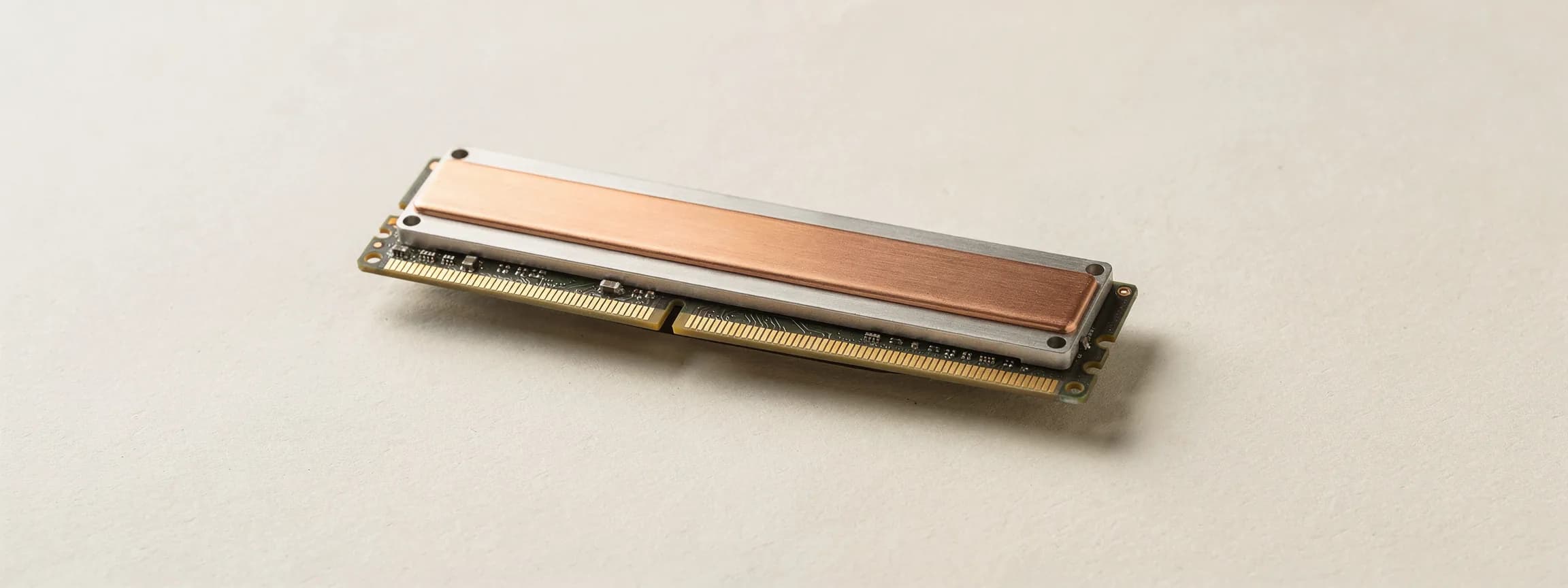
In scope: the memory hierarchy and the memory wall, HBM and DRAM scaling, bandwidth and capacity limits, processing-in-memory, accelerator and NPU architecture, advanced packaging, and interconnect including optical interconnect and co-packaged optics. Memory is the binding constraint of this cycle. Out of scope: photonic compute (computing in light, as distinct from communicating in light) and quantum computing — frontier science with no near-term effect on what a token costs — and consumer buying advice, which is an editorial beat rather than research.


Memory is the wall. A modern accelerator multiplies far faster than it can be fed.
1Eight DRAM dies stacked over one logic die.
So the stack sits directly on the package — eight layers deep, not spread across a board.
2Copper through-silicon vias: the bandwidth path.
And the copper vias thread it vertically. That path is what the price of a token ultimately rides on.
3Cut away at the near corner, so the section is real.
Hardware — Memory & Compute Architecture
The silicon rung of the inference stack, read memory-first. The scope is deliberate: the memory
hierarchy, HBM and DRAM scaling, bandwidth and capacity limits, computing inside memory,
accelerator architecture and the packaging that bolts memory to compute. Computing in light and
quantum computing are out — frontier science with no near-term effect on what a token costs — and
communicating in light belongs to the networking rung, not this one. The organising claim is
Onur Mutlu's: modern machines spend between 60% and 90% of their total system energy moving data
rather than computing on it, and a DRAM read costs roughly 800× a 64-bit floating-point operation
and about 6,400× a 32-bit integer add
(Memory-Centric Computing). On that arithmetic the
memory is the machine and the processor is an accessory.
What this rung prices
A model is quoted per token; a buyer pays for a finished task; and in saturated decode the thing actually being bought in between is memory bandwidth. That is why this rung has a unit of its own — dollars per petabyte of bandwidth delivered — set out in closed form with every parameter stated (accelerator price, a 1.5× system multiplier, four-year straight-line depreciation, PUE 1.3, $0.08/kWh, and a memory-bandwidth utilisation figure of 0.50 to 0.62), so that two fleets of different vintages can be compared without reference to any particular model (close read of Matsuoka 2607.07207). Everything on the rung moves that number in one of three ways: how much bandwidth a stack delivers (HBM generation), how many stacks can be attached to a die at all (packaging), and how much of the energy budget is burned shifting bytes instead of using them (processing in memory). When memory gets scarce, the price of the hardware rises before the price of the token does — and the gap between what an incumbent's already-depreciated fleet costs to run and what a new buyer's fleet costs to run is the wedge that decides who can undercut whom.
The load-bearing findings
- On the paper's own parameters a 2026 new build costs about 3.2× what a depreciated incumbent pays. A GB300-class 2026 build comes out at roughly $0.174 per petabyte moved against a depreciated-H100 incumbent floor of about $0.054, narrowing to 1.9–2.0× in 2027 and re-widening to around 3× (base) or above 4× (shortage branch) by 2029–30 (close read). The mechanism — a depreciation conveyor, where the cost advantage rotates between incumbents by purchase year and never transfers to an entrant inside the horizon — is a structural argument rather than a forecast, and it is the strongest thing in the source. See memory scarcity and inference economics.
- Which purchase year is underwater depends on the pricing regime, and the two regimes cross over. The breakeven grid is 16 cells — four purchase years × two pricing regimes × two HBM branches — read off a bar chart rather than a table. The 2027 cohort clears in all four of its cells (7.5–11.1% of tokens needing premium pricing); the 2026 cohort's worst cell is sticky pricing at about 31.3%, not the coupled regime; the 2029 cohort under coupled-plus-shortage needs about 37.6% (close read). The crossover is real arithmetic — one regime is pegged to a ratio and the other to an absolute — but the 10–20% band those numbers are judged against is asserted in the paper with no source, so the verdict is a function of an unsourced parameter.
- Bandwidth per accelerator is being bought by moving the memory's base die onto a logic process. HBM4 doubles the interface to 2,048 bits and the channel count to 32 per stack, and the base die moves off DRAM processes onto TSMC 12FFC or N5 — about twice as power-efficient as HBM3E's DRAM-based base die — with HBM4E reaching 3 TB/s per stack against HBM3E's 1.2 TB/s (HBM architectural shakeup). NVIDIA's own material puts Rubin at 288 GB of HBM4 at 22 TB/s against Blackwell's 192 GB at 8 TB/s, a 2.8× bandwidth step (Inside the Vera Rubin Platform) — vendor self-reported, and the platform's rack-scale framing is a sales argument as much as a measurement. See HBM4 memory architecture.
- The binding constraint has been packaging, not fabrication, and it is loosening rather than tightening. TSMC's CoWoS capacity went from roughly 35,000 wafers a month in late 2024 to about 75,000 by end-2025 with a 130,000 target for end-2026 (TSMC to quadruple advanced packaging); four months later that target reads as a 120,000–140,000 band, with a further 50,000–60,000 from outsourced assemblers, and the supply-demand gap projected to narrow from about 20% to about 10% by end-2026 (CoWoS gap narrowing). Both are projections carrying explicit as-of dates, not audited output. NVIDIA has reserved the majority of that capacity (NVIDIA snaps up packaging capacity), which is what makes the queue rather than the wafer the thing to watch — advanced packaging and CoWoS.
- The next lithography generation has been priced out, at least for now. TSMC's deputy co-COO said publicly that the company has no current plans to adopt ASML's high-NA EUV tools, at upwards of €350 million each — roughly double the current EUV generation — and that it can produce its first ~1.3nm node without them, relying on process optimisation and GPU-accelerated mask synthesis instead (TSMC delays high-NA EUV; cuLitho collaboration, which is a vendor announcement). The source itself notes the per-tool cost is reported anywhere between $350M and $410M, and that "no current plans" is a deferral rather than a refusal.
- Custom accelerators are growing faster than merchant GPUs without displacing them. TrendForce forecasts 2026 AI server shipments up more than 28% year on year, with ASIC-based systems at 27.8% of shipments — the highest since 2023 — against 69.7% for GPU systems, and the top five North American cloud buyers raising capital expenditure about 40% (TrendForce ASIC share). These are forecasts, not realised shipments, and they are unit shares rather than revenue shares, so the GPU's revenue position sits higher than 69.7% implies. See custom silicon vs GPU.
What we do not know yet
- Nothing on this rung was measured here. Every figure above is read from someone else's document. The bandwidth numbers come from vendor material or analyst houses, the cost model comes from a single-author preprint, and no $/PB figure has been reproduced against a machine anyone here has run.
- The realised CoWoS number has never been checked against the target. The KB carries a 130,000 target, then a 120,000–140,000 band, both projections; the gap-narrowing source says plainly that closing this needs TSMC's own quarterly management report, which the rung has for one quarter (TSMC Q2 2026) but has not reconciled against the capacity claim.
- The most decision-relevant number in the memory model is a judgment, not a computation. The revision of token-demand growth from 4–7× a year to 2–3× is stated immediately after a list of five biases, four of which are given no quantity at all; the author labels even that revised figure an upper bound (close read). The same close read finds a cited 73× spread in realised cost on identical H100 hardware, which if real would swamp the 2–4× vintage effect the whole model is built to discriminate.
- Processing in memory has no shipped economics on this rung. The case for computing inside memory rests on energy ratios and laboratory demonstrations, and the source's own account of the barriers is economic rather than technical — a standards committee of roughly 390 companies and an incumbent industry with no reason to move (Memory-Centric Computing). That source is itself a synthesis of public talks and papers rather than a single fetched document. Near-memory compute appears in the HBM roadmap as a described capability with no worked cost example (HBM shakeup) — processing in memory.
- One memory supplier's picture reaches us with a hole in it. The SK hynix outlook carries the share and capacity figures but records that the article's three named market headwinds were not captured from the search snippet and need re-ingesting (SK hynix 2026 outlook). The memory-scarcity paper cannot fill that gap: it contains no supplier-level analysis at all and treats scarcity as a single exogenous input.
Read next
- memory-scarcity-2607.07207-closeread — the only primary-text read on the rung, and it corrects its own parent ingest on four points.
- memory-centric-computing-mutlu — why the memory, not the processor, is where the energy goes.
- hbm4-c-hbm4e-architectural-shakeup — the generation change that moves bandwidth per accelerator.