Hardware
The silicon rung of the inference stack, read memory-first.
Memory bandwidth of one H100 SXM's 80 GB of HBM3 — the wall the arithmetic waits behind
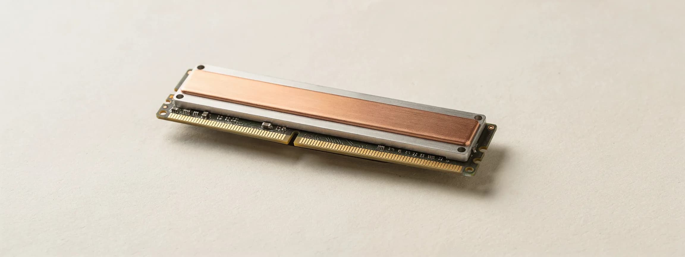
In scope: the memory hierarchy and the memory wall, HBM and DRAM scaling, bandwidth and capacity limits, processing-in-memory, accelerator and NPU architecture, advanced packaging, and interconnect including optical interconnect and co-packaged optics. Memory is the binding constraint of this cycle. Out of scope: photonic compute (computing in light, as distinct from communicating in light) and quantum computing — frontier science with no near-term effect on what a token costs — and consumer buying advice, which is an editorial beat rather than research.


| Type | Source | Published |
|---|---|---|
| ANALYSIS | TSMC Debuts A13 Technology at 2026 North America Technology Symposium TSMC / Industry coverage · TSMC TSMC unveils A13 (1.3nm direct shrink of A14) and N2U process nodes at NA Tech Symposium — A13 production targeted for 2029 for AI/HPC, N2U a more affordable variant for phones/laptops/AI; Arizona advanced packaging facility announced | 2026-04-23 |
| ANALYSIS | TSMC Delays Use of ASML's High-NA EUV Machines Over Cost Concerns Bloomberg · Bloomberg / TSMC / ASML TSMC publicly defers high-NA EUV adoption until at least 2029, citing ~$400M per-machine cost (vs ~$200M for current EUV). Plans to squeeze more performance from existing EUV through process optimization (A13, N2U) — major signal for ASML revenue | 2026-04-22 |
| ANALYSIS | NVIDIA Snaps Up AI Chip Packaging Capacity as TSMC Expands in U.S. CNBC · CNBC / NVIDIA / TSMC NVIDIA has reserved the majority of TSMC's most advanced packaging capacity (CoWoS), making advanced packaging — not fabrication — the next bottleneck for AI accelerator supply | 2026-04-08 |